OTC aims to start mass production of advanced PCBs by October 2025 at its Joetsu Plant.
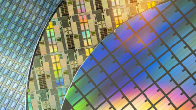
OKI Circuit Technology has successfully developed 124-layer PCB technology for wafer inspection equipment designed for next-generation high bandwidth memory, such as HBM mounted on AI semiconductors. This is a roughly 15% increase in the number of layers over conventional 108-layer designs. OTC is seeking to establish mass production technology by October 2025 at its Joetsu Plant in Joetsu City, Niigata Prefecture, which has a proven track record and advanced development and production capabilities in the field of high multilayer, high-precision, large-format PCBs for semiconductor inspection equipment.
AI processing requires the transmission of vast data volumes between graphics processing unit (GPU) semiconductors and memory. As semiconductor performance increases, the memory installed is also required to have high-speed, high-frequency, and high-density data transfer capabilities. HBM features a stacked DRAM structure, requiring technology capable of fabricating wafers even more thinly and precisely. This configuration also requires that the PCBs used in inspection equipment meet even higher levels of performance and quality.
Since the latest semiconductors process an enormous number of signals and the number of wafer-mounted chips increases due to process miniaturization, it is necessary to increase density and more layers on the PCBs used in inspection equipment. Nevertheless, PCB thickness has been limited to 7.6 mm due to various constraints, and 108 layers was the maximum limit with conventional technology. This time, by developing ultra-thin materials and tools and handling technologies suitable for ultra-thin materials, together with developing and introducing a proprietary automatic transport system for ultra-thin materials into its production line, OTC has successfully developed 124-layer PCB technology with a board thickness of 7.6 mm.
OKI continues to focus on its EMS business, providing manufacturing services that include design, production, and reliability testing. The company emphasizes technology development in the PCB sector and developed this new technology to address expected growth areas such as AI semiconductors, aerospace, defense, robotics, and next-generation communications. OKI plans to further develop PCBs and manufacturing technologies in line with future technological advancements.
Note 1: HBM (High Bandwidth Memory)
Next-generation high-bandwidth memory. Consists of multiple stacked DRAM with a dedicated high-speed interface.
Note 2: DRAM (Dynamic Random Access Memory)
A type of temporary data storage memory widely used in computers and electronic devices, made up of cells consisting of capacitors that hold electric charge and transistors to control this charge. As volatile memory, this memory loses data when power supply is cut off. In addition, it allows for high-speed data read/write and is well-suited for increased capacity. It is used in personal computers, servers, mobile devices, etc.
For more information, visit oki.com.